










IT News on September 29th: TomsHardWare has discovered that Intel publicly released a new patent regarding the CPU packaging earlier this month, proposing the idea of directly integrating Micro LED light bulbs into the processor itself.
This means that in the future, not only can the surface of processors display the RGB lighting effects, but it will also be possible to customize the lighting of Logo or text, or to change the lighting effects in real-time based on the processor's load, temperature, or operating status.
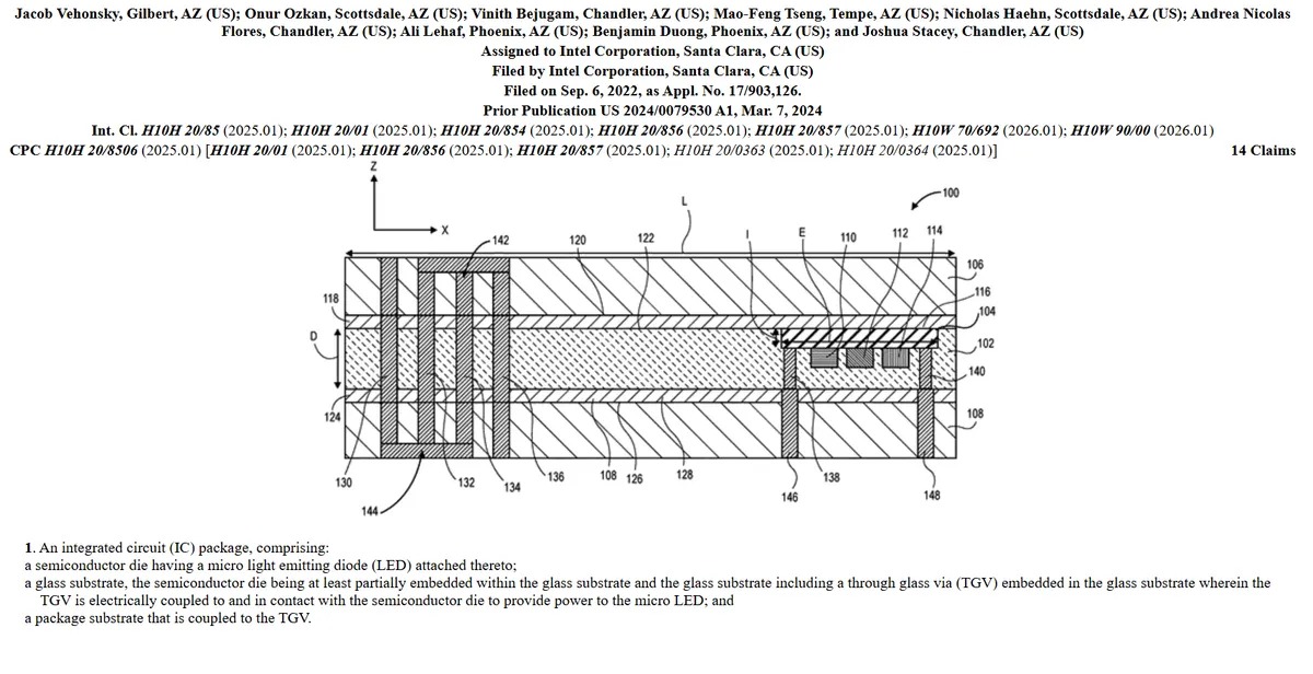
This patent was submitted in 2022 and was officially made public this month. The patent describes an encapsulation scheme based on a glass substrate ( Glass Substrate ) and glass-through holes ( TGV ), which allows the Micro LED light beads to be directly connected to semiconductor dies (with the CPU core being responsible for power supply and signal scheduling). As a result, the lighting on the surface of the encapsulation can change in real-time according to processor load, temperature, or specific instructions.
Intel stated in its patent that these Micro LED can serve as decorative components of electronic devices (used solely to provide dynamic lighting effects), or they can function as indicator lights, changing the lighting effect when the device is performing specific tasks.
One of the more notable ideas is to encapsulate text or logos that light up on the surface at CPU. Intel believes that the text on the processor surface can be made to glow through the use of Micro LED. However, in theory, the vast majority of users will continue to install a cooler after installing CPU. As for how this lighting design will be implemented, Intel has not provided any specific details.
From the public schematic diagrams, it can be seen that the glass substrate is located between two layers of packaging substrates, with the semiconductor die portion embedded within the glass substrate, leaving the back of the die exposed; in other implementation methods, the die can also be completely embedded inside the substrate. Micro LED can be directly connected to the semiconductor die or connected via nanowires, while TGV (glass vias, used to establish vertical electrical connections within the glass substrate) is responsible for transmitting power and signals within the glass substrate.
Intel stated that this packaging structure is constructed using two layers of silicon nitride material and is combined with a glass substrate. In recent years, the company has been continuously advancing the research and development of glass substrate technology and believes that compared to traditional organic substrates, the interconnect density can be increased by about 10 times, which helps to support more complex chip packaging designs.
At present, this technology is still in the patent stage, which does not mean that related products have already entered mass production. The patent submitted by Intel four years ago has now been officially made public. Whether there will be processor products equipped with Micro LED on the market in the future remains to be further observed.
Related Reading:
- Intel Increases Investment in Glass Substrates; New Mexico Factory Aims to Become the World's First Mass-Production Base, Says Report
- AI Chip New Engine: Intel's Debut EMIB Glass Substrate, 78mm Ultra-large Package, 22-layer Stacking
- Intel: There are no changes to the semiconductor glass substrate development plan compared to the 2023 roadmap.